10th IUVSTA school
International Summer School on Physics at Nanoscale
30th May – 4th June 2011
Devět Skal, Czech Republic |
|
Javier Aizpurua: Plasmonic antennas for field-enhanced spectroscopy and microscopy
Nanophotonics Group, Center for Materials Physics
Spanish Council for Scientific Research (CSIC)
The Nanophotonics group at the Center of Materials Physics addresses the optical response of nanoscale
systems.
Some of our topics of interest are:
• Plasmonics
• Metallic nanoantennas
• Near-field microscopy
• Surface-enhanced Raman Scattering
• Quantum dots
• Acousto-plasmonics
• Scanning Transmission Electron Microscopy
• Photons in tunneling microscopy
|
 |
|
[Return to top] |
Thomas Cornelius:
Mechanical behavior of single nanostructures
Research
Thomas Cornelius is a postdoctoral researcher at the ID01 beamline at the European Synchrotron Radiation Facility (ESRF) in Grenoble (France). His research interests are in nanoscale science. He holds a physics degree and PhD from the University in Heidelberg. During his doctoral studies and a postdoctoral fellowship at the Materials Research Department at GSI Helmholtz Centre for Heavy Ion Research in Darmstadt (Germany) he concentrated on the electrochemical growth of metal and semimetal nanowires as well as on the characterisation of their structural, electrical, and infrared optical properties. At ESRF, he focuses on the characterization of the mechanical behavior of single nanostructures. For this, our team at ID01 developed an in situ combination of nanofocused X-ray diffraction and atomic force microscopy.
|
 |
|
[Return to top] |
Markus Etzkorn:
1) Nanostructures and self assembly
2) Nanomagnetism and spin dynamics
Scientific background
- Research stay at the IBM Almaden research center, San Jose (CA), USA.
- Post-Doc at the Ecole Polytechnique Fédérale de Lausanne, Switzerland
- Post-Doc at the Max-Planck-Institute of Microstructure Physics in Halle (Saale), Germany
- Research stay at the CRMCN-CNRS, Luminy, Marseille (France) supported by DAAD, project on self-organized structures in SiC.
- PhD-student at the Max-Planck-Institute of Microstructure Physics in Halle (Saale), Germany
- Diploma thesis at the Ruhr-Universität Bochum, Germany. Subject: Unidirektionale
Austauschanisotropie in ferromagnetischen und antiferro-magnetischen Schichten
- Study of physics at the Ruhr-Universität Bochum, Germany
Web page |
 |
|
[Return to top] |
|
Olivier Fruchart: A short dive into nanomagnetism and spin electronics
Olivier Fruchart is currently working in Institut Néel (CNRS) in Grenoble, as a scientist (permanent position). His research interest is to fabricate novel nanometer-sized magnetic objects by tailoring UHV epitaxial self-organization processes on surfaces. Due to their high structural and chemical quality, these systems can serve as model systems for magnetic studies. These studies include magnetism at interfaces, micromagnetism (magnetic domains, magnetization reversal, etc.), interplay of structure and magnetism, etc.
Study on Semiconductor Nanostructures nanoparticles, Study on Molecular Electronics
exciton etc.
Institut Néel (CNRS & UJF) - Building D
25 rue des Martyrs
BP166 - 38042 Grenoble Cedex 9 (France) |
 |
|
[Return to top] |
|
Hong-Jun Gao: Nanoscale electronic devices
Dr. Hong-jun Gao got his Ph.D. is now a professor and Deputy-Director of the Institute of Physics, Chinese Academy of Sciences. Since 2001, he has served as the Director of Nanoscale Physics and Device Laboratory, Institute of Physics, CAS. Dr. Gao is a Fellow of the Institute of Physics, UK, and has served as an Associate Editor for Appl. Phys. Lett. Since 2010 and an editorial board member for the New Journal of Physics since 2003. He was the Scientific Secretary of the International Union of Vacuum Science, Technology, and Applications (IUVSTA) in the triennium 2004-2007, Vice-Chairman of the Nano Science and Technology Division (NSTD), IUVSTA in the triennium 2007-2010, and is now the Chairman of the NSTD, IUVSTA (2010-2013). From 1997 to 2000, he worked at the Oak Ridge National Laboratory (ORNL) as a Guest Scientist on structures and properties of nanomaterials. In recent years he visited several universities in the US and Germany as a Visiting Professor, and ORNL as Scientific Consultant several times.
His research interests are in surface/interface structure and physical properties with scanning tunneling microscopy/spectroscopy (STM/STS) including molecules at solid surfaces at a single molecular level, and nano-materials and nano-electronic devices. He has 6 international books/chapters and about 200 journal publications including 6 international invited review articles and 15 PRL, 7 JACS, and 10 Adv. Mater., and 16 APL papers. His research on the construction of an anchored single molecular rotor array, and on nanorecording using conductance transition at a single molecular scale, have been highlighted by the American Physical Societyphysics, Physical Review Focus, Science News, Nature Materials, and Nature Nanotechnology. In 2008 and 2009, he was awarded the OCPA AAA (Robert) Prize (OCPA: the Overseas Chinese Physics Association; AAA: Achievement in Asia Award), the TWAS Prize in Physics 2009 (TWAS: Third World Academy of Sciences), and Humboldt Research Award 2010. |
 |
|
[Return to top] |
|
Franz Giessibl:
Study of surfaces by atomically resolved AFM
Franz Giessibl is currently full Professor at Universität Regensburg, Naturwissenschaftliche Fakultät II - Physik, Institut für Experimentelle und Angewandte Physik.
1981 - 1982: University of Applied Sciences Munich, Microengineering, Prediploma
1982 - 1988: Technical University Munich and Federal Institute of Technology Zurich, Physics, Diploma thesis with Prof. Dr. Gerhard Abstreiter in experimental semiconductor physics
1988 - 1992: Ludwig-Maximilians-University Munich / IBM Research Group Munich
Dr. rer. nat. in experimental physics with Prof. Dr. Gerd Binnig in Atomic Force Microscopy
2001: Universität Augsburg, Habilitation, Habilitation-thesis "Progress in Atomic Force Microscopy" (2000)
Professional experience:
1981 - 1988: Numerous summer jobs with International Business Machines Corporation, Max Planck Institut and others
1992: Postdoctoral Fellow IBM
1992 - 1994: Park Scientific Instruments Inc., Sunnyvale, California: UHV R&D Scientist, Senior Scientist and Director of UHV Products
1995 - 1996: McKinsey&Company, Inc.: Senior Associate
1996 - 2006: Universität Augsburg, Experimentalphysik VI: Leader scanning probe microscopy group and lecturer
2006 - today: Full Professor at Universität Regensburg, Naturwissenschaftliche Fakultät II - Physik, Institut für Experimentelle und Angewandte Physik
Awards:
1994: R&D 100 Award
2000: Deutscher Nanowissenschaftspreis
2001: Eudolf-Kaiser-Preis
2009: Karl Heinz Beckurts-Preis |
 |
|
[Return to top] |
| Ivan Gordon: Thin film solar cells research: where nanotechnology meets photovoltaics
Manager of the Photovoltaics Explore group, IMEC, Leuven, Belgium
Dr. Ivan Gordon received his Master Degree in Physics in 1997 from the University of Leuven (KUL), Belgium. He did his PhD research in the field of novel magnetic materials for sensor applications and obtained his PhD Degree from the University of Leuven in February 2002. He started to work at imec in June 2003 in the photovoltaics department, where he is currently the head of the Photovoltaics Explore group, working on thin-film silicon solar cells, CIGS solar cells, III-V solar cells, a-Si/c-Si heterojunction solar cells and advanced module concepts for thin c-Si wafer-based cells. Since 2008, he is associate editor for the international scientific journal Solar Energy Materials and Solar Cells. He has authored and co-authored more than 100 journal and conference papers.
|
 |
|
[Return to top] |
|
Pavel Jelínek: Exploring Nano: what can we learn/expect from theoretical studies?
Research topics:
- Development of ab-initio fast local orbital DFT FIREBALL code (http://fireball-dft.org)
- Theoretical description of SPM methods (single atom manipulations, dissipative mechanism at atomic scale, chemical identification, imaging processes).
- Ab initio simulations of the mechanical, optical and transport properties of nanostructures.
- AFM/STM experiments with atomic resolution.
- Theoretical simulations of non-adiabatic processes
|
 |
|
[Return to top] |
|
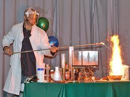
Michael Londesborough: Energy - its role and resources
Dr. Michael Londesborough, Ph.D. is a British-Czech scientist, who moved in the Bohemia in 2002. He is currently producing the feature called "Michael's experiment" on the TV periodical CT PORT. He has been conducting research during last five years in the Institute of Inorganic Chemistry of the Academy of Sciences of the Czech Republic in Rez. Michael is cooperating in the projects with the British Council in Prague, participating in popularization projects of the Academy of Sciences, Czech TV and National Technical Museum.
|
 |
|
[Return to top] |
Lars Montelius: Nanowires for life science applications
Prof, Head Exploratory Nanotechnology
Nanometer Structure Consortium
Lund University, Solid State Physics,
Sweden
Lars Montelius, Professor in Nanotechnology at nmC@LU, Lund University, Sweden. LM is also acting President Swedish Vacuum Society & Swedish Councillor of IUVSTA (International Union of Vacuum Science & Technology). His 20 years of work in nanotechnology has centered around scanning probe microscopy & spectroscopy & luminescence & imaging & manipulation of low-D structures, electron & ion beam and nanoimprint lithography & processing applied to single electron tunneling, quantized conductance and various bio and NEMS-devices. His recent research interests are on exploratory nanotechnology bringing it to the life sciences, especially in the neuronanosciences. LM has published more than 140 articles, given more than 65 invited talks and has filed 20 patents. LM is also the founder of several companies working with nanotechnology and a Director of the Nanoimprimt Lithography company Obducat AB, Sweden. Between Jan 2009 – Feb 2011, he was appointed director for Øresund University & Øresund Science Region, being a cross-border cooperation between eleven universities, three regional authorities, two countries in the Øresund Region, one of Europes most innovative regions.
|
 |
| [Return to top] |
Walter Riess:
The Future of Nanoelectronics
Department Head, Science & Technology
IBM Research GmbH, Zürich Research Laboratory, Switzerland
Dr. Walter Riess studied Physics at the University of Bayreuth, Germany, where he received a Master degree (Physics) in 1987 and a Ph.D. (Physics) in 1991. From 1991 to 1995, he was leading the Polymeric Light-Emitting Device Group at the Lehrstuhl Experimental Physik II at the University of Bayreuth.
In 1996 the University of Bayreuth conferred Walter Riess the habilitation based on his thesis on polymeric light-emitting diodes.
In 1995 he joined the IBM Zurich Research Laboratory as a Research Staff Member and in 1998 Dr. Riess became manager of the Display Technology Group working on display applications of electroluminescent organic materials.
From 2004 to 2008 Dr. Riess was leading the Nanoscale Structures and Devices group where his research activities focused on ultimate and beyond CMOS devices based on semiconducting nanowires.
Since November of 2008, Dr. Riess has been the Department Head of the Science & Technology Department at the IBM Zurich Research Laboratory. Research activities in the department span: chip cooling, advanced thermal packaging, optical interconnects, silicon photonics, nanofabrication, 3D integration, self-assembly and patterning, experimental biology, magnetism, spintronics, AFM & STM imaging, III-V and Ge on silicon, semiconducting nanowires and molecular electronics.
In 2005 Dr. Riess was recognized with IBM’s Corporate Patent Portfolio Award and in 2007 he received a Special Recognition Award from the Society for Information Display for his leading contributions to the design and development of top-emitting large area active matrix organic light emitting display driven by amorphous-silicon thin film transistors.
Dr. Riess holds more than 40 patents. He is a member of the German Physical Society, the Swiss Physical Society, IEEE and the Materials Research Society.
http://www.zurich.ibm.com
|
 |
| [Return to top] |
|
Jens Schneider :
1) "Reality is a bitch" - from lab to production
2) Crystalline Silicon on Glass - a unique challenge
for thin film PV
Since 2008 Paper Review Expert for EUPVSEC
Since 2005 Process Development Engineer at CSG Solar AG, Thalheim, Germany
2005 PhD in Electrical Engineering from University of Technology, Berlin on
'Nucleation and growth during the formation of polycrystalline silicon thin films'
2002 Diploma in Electrical Engineering from University of Technology, Berlin
Scientific interest
Photovoltaics
Polycrystalline Silicon Thin Films
Solar cell performance limiting mechanisms in pc-Si thin film Solar cells
|
 |
| [Return to top] |
|
Markus Schubert:
1) Photovoltaics 2011 in Germany, worldwide, and at small ipe
2) Direct optical detection of biolayers, plus a brief history of subretinal implants
Institut für Photovoltaik, Stuttgart University
Markus B. Schubert holds a Dipl.-Ing. and a Dr.-Ing. degree, both obtained from the Faculty of Electrical Engineering at the University of Stuttgart. He received his Dipl.-Ing. degree in 1985, and worked as a research assistant at Stuttgart University, Institute of Physical Electronics (ipe) on thin film deposition and the structural, optical and electronic characterization of amorphous semiconductors. He received his Dr.-Ing. degree on Raman scattering in amorphous semiconductors in 1992. In 1992 to 1996, in addition to ipe occupation, he was a professor with the Faculty of Engineering Sciences at the University of Ulm (Germany), lecturing on the fundamentals of energy conversion. Since 1993, he has been leading a work group at ipe, managing various research projects on thin film sensors and solar cells. From 2002 to 2005, he overheaded all silicon work at ipe, covering topics from amorphous thin films to wafer based solar cells and microelectronics. His favourite research topics include materials research and development of silicon solar cells, photovoltaic systems' technology and yield analyses, as well as thin film photodetectors for retina implants, high definition Thin-Film-on-CMOS cameras, and microsystems for biodiagnostics. He has authored and coauthored more than 150 publications. Since 1999, Markus Schubert serves as Associate Director of the ipe (40 employees, 5 research groups, cf. http://www.ipe.uni‑stuttgart.de), assisting the Director Prof. Jürgen H. Werner. M. Schubert is a member of several scientific and engineering organisations, and of the technical committee on sensors of the VDE/VDI GMM engineering society.
|
 |
| [Return to top] |
|
Christian Teichert
1) Nanostructure characterization by AFM
2) Electrical characterization by conductive AFM
Born in 1960 in Halle, Germany. Christian Teichert is currently working as an associate professor in material physics, Institute of Physics, Montanuniversitat Leoben. Teacher, student's supervisor, organizer of numerous conferences and workshops. Since 2004 he is representative for Austria and (since 2010) Secretary of the Nanometer Structure Division of the IUVSTA.
Research interests:
Self-organization of semiconductor nanostructures in heteroepitaxy and under ion erosion; pattern formation and growth modes in crystalline organic thin films; nanometer scale investigation of electrical properties of thin films using conductive AFM, photoconductive AFM, friction force microscopy, transverse shear microscopy and piezoresponse force microscopy; in situ growth investigations with XPEEM and LEEM, magnetic nanostructures; scanning probe microscopy investigations of surface roughness from hard coatings to biomaterials, correlation between nanomorphology and wetting behavior of solid surfaces
|
 |
|
[Return to top] |
|
Klaus Wandelt: Surface Science of Metal/Electrolyte Interfaces
Professor and Director at Institute of Physical and Theoretical Chemistry of Bonn, Germany
University Bonn
Wegeler Str. 12
53115 Bonn Germany
Research interest:
Physics and chemistry of solid surfaces in contact with vacuum, gases and electrolytes, in particular, adsorption on metal and alloy surfaces, heteroepitaxial metal films and surface alloys, oxide films and ionic crystal surfaces, atomic structure and self-assembled organic layers at metal/electrolyte interfaces, growth and structure of epicuticular wax layers (“green surface science”).
More than 400 original publications and 7 edited books and monographs. More than 1200 invited and plenary talks, oral and poster presentations at conferences as well as colloquia and seminars.
|

|
|
|
|
[Return to top] |
[Return to top] |
|
|
|
|